

SMD Desoldering Machine Automatic Hot Air
SMD Desoldering Machine Automatic Hot Air From China Shenzhen Factory.
Aprašymas
SMD Desoldering Machine Automatic Hot Air
The SMD Desoldering Machine is an automatic tool that uses hot air to remove surface mount components
from a printed circuit board. The machine is designed to heat the solder joints of the component, making it
easy to lift off the board without damaging the board or the component.
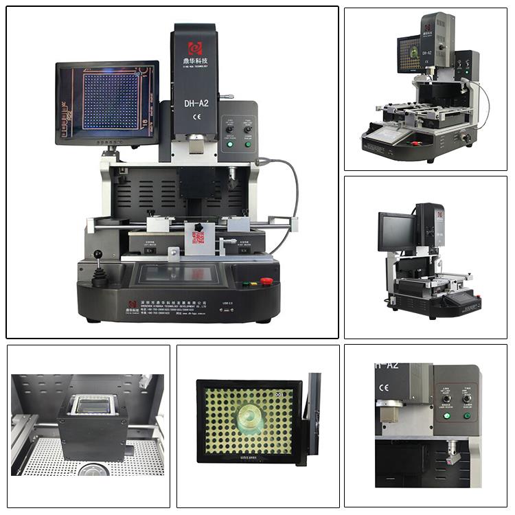

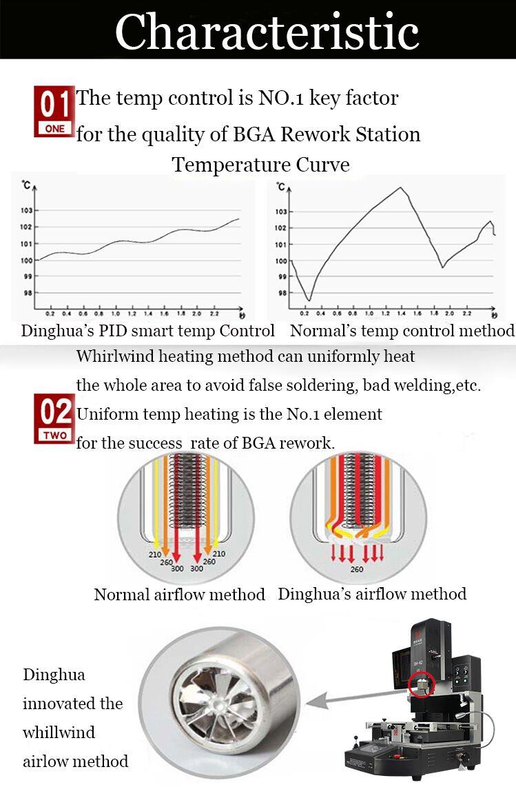
1.Application Of SMD Desoldering Machine Automatic Hot Air
Solder, reball, desoldering different kind of chips: BGA,PGA,POP,BQFP,QFN,SOT223,PLCC,TQFP,TDFN,TSOP,
PBGA,CPGA,LED chip.
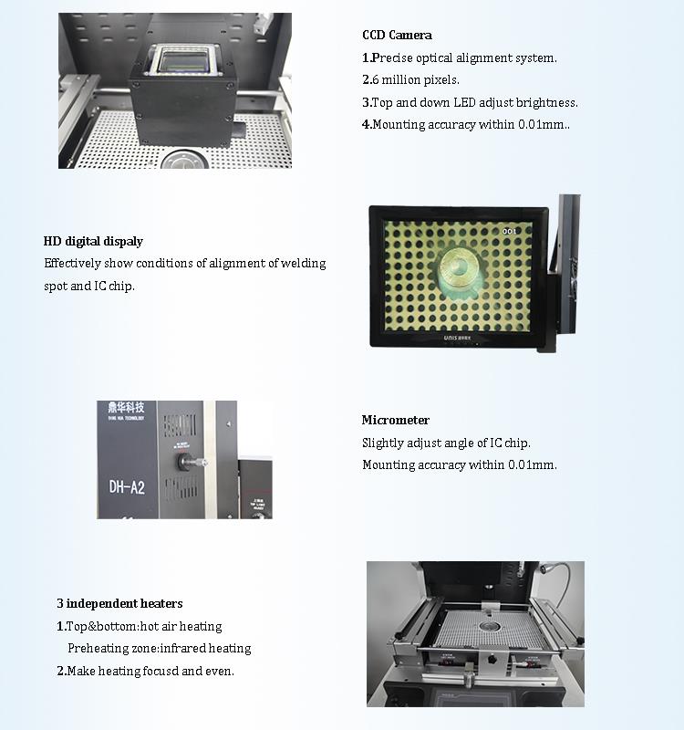
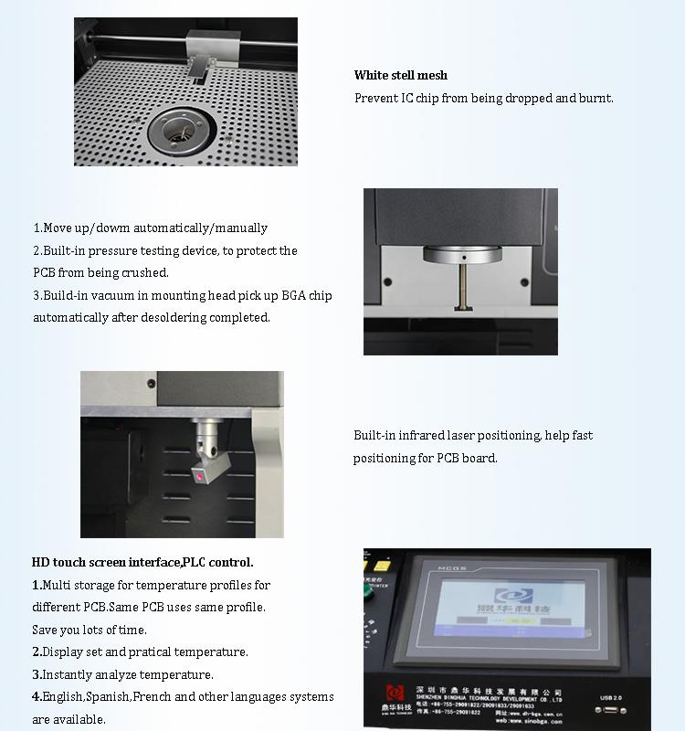
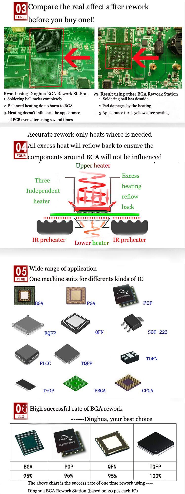
2.Product Features of laser position SMD Desoldering Machine Automatic Hot Air

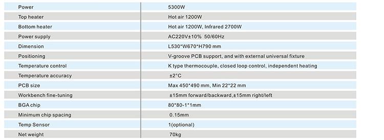
3.Specification of laser positioning SMD Desoldering Machine Automatic Hot Air
4.Details of SMD Desoldering Machine Automatic Hot Air

5.Why Choose Our Infrared SMD Desoldering Machine Automatic Hot Air?
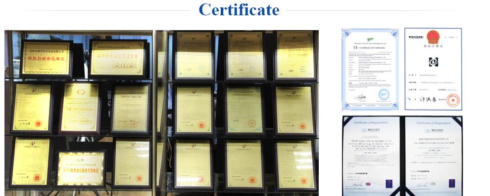
6.Certificate of Optical Alignment SMD Desoldering Machine Automatic Hot Air
UL, E-MARK, CCC, FCC, CE ROHS certificates. Meanwhile, to improve and perfect the quality system,
Dinghua has passed ISO, GMP, FCCA, C-TPAT on-site audit certification.
7.Packing & Shipment of CCD Camera SMD Desoldering Machine Automatic Hot Air

8.Shipment for SMD Desoldering Machine Automatic Hot Air Split Vision
DHL/TNT/FEDEX. If you want other shipping term, please tell us. We will support you.
9. Terms of Payment
Bank transfer, Western Union, Credit Card.
Please tell us if you need other support.
10. Operation guide for SMD Desoldering Machine Automatic Hot Air
11.Contact us for SMD Desoldering Machine Automatic Hot Air
Email:John@dh-kc.com
MOB/WhatsApp/Wechat: +15768114827
Click the link to add my WhatsApp:
https://api.whatsapp.com/send?phone=8615768114827
12. Related knowledge of SMD Desoldering Machine Automatic Hot Air
Precautions for PCB board copper plating
Pcb circuit board design and production have a certain process and precautions, pcb circuit board copper
is a crucial step in the pcb design, with a certain technical content, then how to do this part of the design
work, I The senior engineers of the company discussed and summarized the following points, hoping to br-
ing benefits to everyone.
Copper coating introduction:
The so-called copper coating is to use the unused space on the PCB as the reference surface, and then fill it
with solid copper. These copper areas are also called copper filling. The significance of copper clad is to red-
uce the ground line impedance, improve the anti-interference ability; reduce the voltage drop, improve the
power supply efficiency; connect with the ground wire, and also reduce the loop area. Also for the purpose
of making the PCB soldered as much as possible, most PCB manufacturers will also require the PCB design-
er to fill the copper or grid-like ground wire in the open area of the PCB. If the copper is not handled proper-
ly, it will If you don’t appreciate it, is it that “benefits outweigh the disadvantages” or “does more harm than
good”?
Everyone knows that at high frequencies, the distributed capacitance of the wiring on the printed circuit bo-
ard will work. When the length is greater than 1/20 of the corresponding wavelength of the noise frequency,
an antenna effect will occur and the noise will be emitted through the wiring. If there is a poorly grounded co-
pper in the PCB, copper is a tool for propagating noise. Therefore, in high-frequency circuits, don't think that
somewhere on the ground is grounded. This is the ground. "Line" must be made with a hole on the wiring at a
pitch less than λ/20, and "good grounding" with the ground plane of the multilayer board. If the copper coatin-
g is properly treated, the copper cladding not only has an increased current, but also plays a dual role of shield-
ing interference.
In copper cladding, in order to achieve the desired effect of copper cladding, there are some issues to be aware
of in copper cladding:
If the PCB has more ground, there are SGND, AGND, GND, etc., according to the difference of PCB board po
-sition, the most important "ground" as the reference reference to separate copper, digital ground and analogg-
round Separate copper to cover, and at the same time, before the copper coating, first increase the corresp-
onding power connection: 5.0V, 3.3V, etc., thus forming a plurality of different shapes of multi-deformation st-
ructure.
2. For single-point connections to different places, the method is to connect through 0 ohm resistors or magnetic
beads or inductors;
3. The copper near the crystal oscillator, the crystal oscillator in the circuit is a high-frequency emission source, t-
he method is to surround the crystal copper, and then the crystal casing is grounded separately.
4. The problem of isolated islands (dead zones), if you feel great, it will not cost much to define a hole in the hole.
5. When starting the wiring, the ground wire should be treated equally. When the wire is routed, the ground wire
should be taken well. It is not possible to rely on the copper to add the via hole to eliminate the ground pin. This h-
as a bad effect.
6. It is best not to have sharp corners on the board ("180 degrees"), because from the electromagnetic point of vi-
ew, this constitutes a transmitting antenna! For other things, there will always be an impact on whether it is big or
small. However, I recommend using the edge of the arc.
7. The wiring of the middle layer of the multi-layer board is not covered with copper. Because it is very difficult for
you to make this copper "good grounding"
8. The metal inside the equipment, such as metal radiators, metal reinforcement strips, etc., must achieve "good g-
rounding".
9. The heat-dissipating metal block of the three-terminal regulator must be well grounded. The grounding isolation
strip near the crystal must be well grounded. In short: the copper on the PCB, if the grounding problem is dealt with,
it must be "profits outweigh the disadvantages", it can reduce the return area of the signal line, and reduce the exter-
nal electromagnetic interference of the signal.
Other related articles include "How is the corrosion of pcb circuit board?" "PCB circuit board manufacturing and pa-
ckaging process" PCB board design and production require a certain amount of technical content, so if you want to
do this well, you need to learn through continuous learning. With the accumulation of experience, we can slowly pl-
an for it.


